RF PCB design can feel like regular PCB design after it drank three espressos and started arguing with physics. At low frequencies, a trace is often treated like a simple copper connection. At radio frequencies, that same trace becomes a transmission line, a tiny antenna, a source of reflections, and sometimes the reason your prototype behaves beautifully on Monday and mysteriously misbehaves on Tuesday.
The good news is that RF PCB design is not magic. It is a disciplined way of controlling energy: where it travels, how it returns, how much it radiates, how much it loses, and how politely it behaves around neighboring circuits. Whether you are building a Bluetooth device, Wi-Fi module, GPS receiver, LoRa sensor, RF amplifier, antenna board, or microwave front end, the same core principles show up again and again: controlled impedance, solid grounding, smart stack-up design, proper materials, short RF paths, careful component placement, and real-world testing.
This simple guide explains RF PCB design in plain English, with enough depth to help you avoid the classic mistakes that turn a promising board into a tiny copper-based headache.
What Is RF PCB Design?
RF PCB design is the process of laying out printed circuit boards that carry radio-frequency signals. These signals may range from a few megahertz to several gigahertz or higher, depending on the application. In this frequency range, the board is no longer just a mechanical platform for components. It becomes part of the circuit.
That is the first big mental shift. In RF design, copper trace width, dielectric thickness, laminate material, solder mask, vias, ground planes, connectors, bends, clearances, and component pads all influence performance. A trace that is “close enough” in a low-speed board might create impedance mismatch, insertion loss, return loss, radiation, or unwanted coupling in an RF board.
For example, a 50-ohm RF trace is not 50 ohms because someone printed the number on the schematic. It becomes 50 ohms because the trace geometry, dielectric constant, copper thickness, and reference plane relationship create that characteristic impedance. Change the board stack-up, and the impedance changes. Change the laminate, and it changes again. RF design rewards consistency and punishes guesswork with impressive enthusiasm.
Why RF PCB Design Is Different From Regular PCB Layout
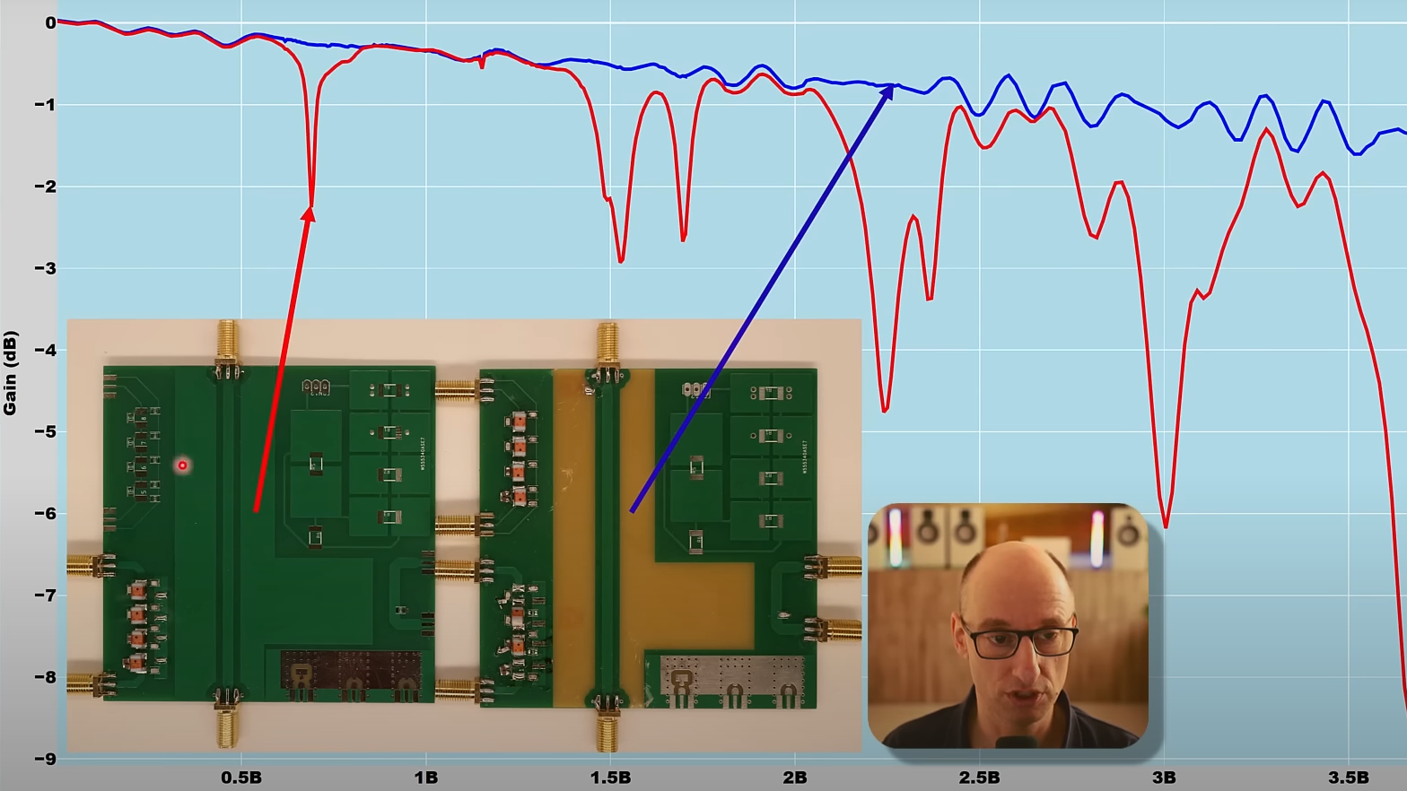
In a low-frequency circuit, current often appears to follow the obvious copper path. In RF circuits, the return current wants to flow directly under the signal path on the nearest reference plane. If that reference plane is interrupted by a split, slot, careless via, or awkward routing decision, the return path spreads out. When the return path spreads, loop area increases. When loop area increases, radiation and noise problems tend to appear. This is the PCB version of leaving breadcrumbs for EMI goblins.
RF design is also more sensitive to impedance discontinuities. A connector launch, via transition, component pad, trace width change, sharp bend, or poorly designed matching network can reflect energy back toward the source. Reflections reduce power transfer and can distort signals. In transmitters, that may mean wasted power and heat. In receivers, it may mean weaker sensitivity. In both cases, the result is usually more debugging and less joy.
Another key difference is material behavior. Standard FR-4 may work for many lower-frequency or cost-sensitive RF projects, but its dielectric constant and loss can vary more than specialized RF laminates. At higher frequencies, low-loss materials with stable dielectric properties become important because the board material directly affects signal speed, attenuation, impedance, and phase behavior.
Start With the RF Requirements Before Drawing Traces
Before opening the PCB editor, define the important electrical requirements. RF boards do not like “we will figure it out later” energy. Start with the operating frequency, bandwidth, transmit power, receiver sensitivity goals, target impedance, acceptable loss, antenna type, connector type, board size, layer count, environment, and manufacturing budget.
A small 915 MHz IoT sensor has different needs than a 5 GHz Wi-Fi board or a microwave amplifier. A simple RF module breakout may survive with a carefully designed 2-layer board, but a compact mixed-signal radio with digital processors, switching regulators, antennas, filters, and amplifiers will often need a 4-layer or higher stack-up with strong isolation and controlled impedance.
At this stage, choose whether your RF paths will use microstrip, stripline, grounded coplanar waveguide, or another transmission-line structure. Microstrip traces are routed on an outer layer over a reference plane. Stripline traces are buried between reference planes. Grounded coplanar waveguide adds ground copper beside the signal trace and is common in RF layouts because it can provide useful field control and convenient grounding.
Choose the Right PCB Stack-Up
The stack-up is the foundation of RF PCB design. A common 4-layer RF-friendly structure is signal on Layer 1, solid ground on Layer 2, power on Layer 3, and signal or low-speed routing on Layer 4. This arrangement gives RF traces on the top layer a nearby continuous ground reference, which helps control impedance and return current.
The distance between the RF trace and its reference plane strongly affects trace width for a given impedance. If the dielectric is thick, the trace may need to be wider to hit 50 ohms. If the dielectric is thin, the trace may become narrower. This is why stack-up should be confirmed with the PCB fabricator early. Do not design a beautiful 50-ohm trace using imaginary dielectric thickness from a random online calculator and then discover that your manufacturer uses a different construction. That is not engineering; that is copper roulette.
For higher-frequency or lower-loss applications, consider RF laminates from established material suppliers. Important material properties include dielectric constant, dissipation factor, dielectric thickness tolerance, thermal stability, copper roughness, and availability. Low-loss materials are usually more expensive than standard FR-4, but they can reduce attenuation and improve predictability when frequency rises.
Controlled Impedance: The Heart of RF Routing
Most RF systems use standard impedance values, with 50 ohms being the most common for single-ended RF paths. The goal is to keep the source, transmission line, connectors, filters, amplifiers, switches, antennas, and test equipment working in the same impedance environment. When impedance changes suddenly, some energy reflects. When reflection increases, return loss gets worse. When return loss gets worse, your RF performance starts writing dramatic poetry.
Controlled impedance is achieved through geometry and materials. Trace width, copper thickness, dielectric height, dielectric constant, solder mask, and neighboring copper all matter. For grounded coplanar waveguide, the gap between the signal trace and side ground pours also affects impedance. For differential RF or high-speed signals, spacing between paired traces affects differential impedance.
Use a field solver or impedance calculator based on the actual stack-up from your fabricator. Better yet, ask the fabricator for recommended trace widths and clearances for your target impedance. For production boards, use impedance test coupons when appropriate. A controlled impedance requirement is only useful when it is tied to real manufacturing data.
Keep RF Traces Short, Direct, and Boring
In RF PCB design, boring is beautiful. Short traces reduce loss, radiation, and opportunities for mismatch. Direct routing reduces surprises. Consistent geometry keeps impedance stable. Avoid unnecessary bends, stubs, via transitions, and layer changes. If a trace must bend, use gentle bends or mitered corners rather than sharp 90-degree turns, especially at higher frequencies.
Place RF components in the order of signal flow. For example, in a receiver path, the antenna connector, matching network, filter, low-noise amplifier, mixer, and related components should be arranged so the RF signal does not wander around the board like it is searching for snacks. Every extra millimeter can add loss, coupling, or phase shift.
Component pads also matter. A tiny capacitor or inductor in a matching network is not ideal by default. Its pad geometry, via placement, and connection style affect parasitic inductance and capacitance. At RF frequencies, the footprint is part of the component. Use manufacturer-recommended land patterns and keep matching network layouts compact and symmetrical.
Grounding: Give Return Current a Clean Path Home
A continuous ground plane is one of the most important features of a successful RF PCB. It provides a stable reference, supports controlled impedance, reduces loop area, and helps contain fields. Avoid routing RF traces over splits, voids, cutouts, or gaps in the reference plane. If the return current cannot flow directly under the signal trace, it will find another path, and that path may not be friendly.
Use plenty of ground vias around RF sections, especially near coplanar waveguide ground pours, connectors, filters, shields, and transitions. Via stitching helps connect top-layer ground copper to internal ground planes and reduces parasitic effects. The exact spacing depends on frequency, wavelength, board geometry, and design goals, but the principle is simple: keep RF ground low-inductance and continuous.
Do not treat ground as a decorative copper flood. Ground copper only helps when it is well connected. A lonely island of copper with no vias can become a resonant troublemaker. If you pour ground near RF traces, stitch it properly. If you cannot stitch it properly, think carefully before leaving it there.
Manage RF Vias Carefully
Vias are useful, but in RF design they are not free. A via adds inductance, capacitance, and possible impedance discontinuity. At lower RF frequencies, a via may be harmless enough. At higher frequencies, via transitions require more careful design. A poorly designed via can increase return loss, reduce bandwidth, and create radiation.
Whenever possible, keep critical RF signals on one layer. If a layer transition is unavoidable, use a controlled via transition with nearby ground vias to provide a clean return-current path. For very high-frequency boards, consider back-drilling, blind vias, buried vias, or optimized launch structures if the application justifies the cost.
Connector launches deserve special attention. SMA, U.FL, MMCX, board-edge, and coaxial launches should be designed using proven manufacturer recommendations or simulated structures. The transition from connector to PCB trace is a common place for mismatch, and it can ruin an otherwise careful RF layout.
Separate RF, Digital, Power, and Noisy Circuits
RF circuits are sensitive. Switching regulators, fast digital buses, clocks, displays, motors, and high-current power paths are noisy. Putting them too close together is like seating a librarian next to a marching band. Something will complain.
Use thoughtful floor planning. Keep the RF front end away from switching power supplies and fast digital edges. Route clock lines and high-speed digital traces away from antennas, low-noise amplifiers, mixers, and matching networks. Use ground shielding, via fences, and physical separation when needed. Place filters where they can do their job before noise spreads into sensitive areas.
Power supply design also matters. RF amplifiers, mixers, oscillators, and synthesizers often need clean supply rails. Use proper decoupling close to device pins, with short connections to ground. Choose capacitor values based on the device manufacturer’s recommendations and the frequency range of interest. A decoupling capacitor placed far away is not a decoupling capacitor; it is mostly a motivational poster.
Design the Antenna Area With Respect
If your RF PCB includes an onboard antenna, the antenna area may be the most sensitive part of the design. Chip antennas, PCB trace antennas, inverted-F antennas, and ceramic antennas all need proper clearance, ground reference, matching, and placement. Follow the antenna manufacturer’s layout exactly whenever possible.
Do not place copper, batteries, metal shields, screws, displays, connectors, or plastic features in the antenna keep-out area unless the antenna design specifically allows it. The enclosure can also detune the antenna, especially if it contains metal or sits very close to the radiator. A board that tests well on the bench may perform differently inside the final product enclosure.
Always include a matching network between the RF output and antenna when recommended. Even if the first prototype uses default component values, the matching network gives you a practical way to tune performance after measuring the assembled product.
Simulate, Review, and Measure
RF PCB design benefits from simulation, but simulation is not a substitute for measurement. Use impedance tools, electromagnetic simulation, and circuit simulation where practical. These tools can help estimate impedance, coupling, insertion loss, return loss, and field behavior before fabrication.
Before releasing the board, perform a layout review focused specifically on RF risks. Check trace impedance, reference planes, ground via placement, connector launches, antenna keep-outs, matching networks, component orientation, power supply filtering, layer transitions, and manufacturability. This review should happen before the board is sent out, not after the courier delivers a box of expensive lessons.
After fabrication, measure the board. A vector network analyzer can evaluate return loss, insertion loss, impedance match, filters, antennas, and RF paths. A spectrum analyzer can help inspect output power, harmonics, spurs, and unwanted emissions. Time-domain reflectometry can help find impedance discontinuities. Real RF performance must be verified in the physical world, because the physical world is where your customers live.
Common RF PCB Design Mistakes
Routing RF Traces Over Broken Ground
This is one of the fastest ways to create noise, radiation, and impedance problems. Keep a continuous reference plane under RF traces.
Changing Trace Width Without a Reason
Trace width changes create impedance transitions. If a taper or transition is needed, design it intentionally instead of letting the layout tool improvise.
Using Random Stack-Up Assumptions
RF impedance depends on real material and geometry. Confirm stack-up details with the fabricator early.
Ignoring Component Parasitics
At RF frequencies, capacitors, inductors, pads, vias, and traces all have parasitic behavior. Use RF-rated components and compact footprints.
Skipping Measurement
A board can look perfect on screen and still fail in the lab. RF design should be tested, tuned, and validated.
Practical Example: A Simple 2.4 GHz RF Board
Imagine a small 2.4 GHz wireless sensor. The design includes a microcontroller, RF transceiver, crystal, matching network, chip antenna, battery connector, and a switching regulator. A good layout begins by placing the RF transceiver close to the antenna feed. The matching network sits between the RF pin and antenna, with extremely short connections. The antenna follows the manufacturer’s exact keep-out and ground recommendations.
The top layer carries the RF trace as a controlled-impedance line. The second layer is a solid ground plane. Ground vias surround the RF path and connect top-layer ground pours to the internal ground plane. The switching regulator is placed away from the RF section, and its inductor is oriented and located to reduce coupling. Digital lines are routed away from the antenna and RF input. Decoupling capacitors sit close to power pins with short ground returns.
After assembly, the antenna match is measured in the final enclosure. The matching components are adjusted if needed. This is a realistic RF workflow: design carefully, build intelligently, measure honestly, and tune based on evidence.
Experiences and Field Lessons From RF PCB Design
One of the most useful lessons in RF PCB design is that small things are not always small. A short stub, a via placed a little too far from ground, a slightly different capacitor package, or a changed dielectric thickness can shift performance in ways that surprise beginners. RF design teaches humility quickly. It also teaches that a checklist is not boring; it is protective armor.
In practical projects, many RF problems begin before routing starts. The schematic may look fine, but the board may not have enough room for proper RF placement. A designer may choose a tiny enclosure, squeeze the antenna into a corner, place a battery beside it, and then wonder why range is poor. The antenna is not being dramatic. It is responding to physics. Giving the RF section enough physical space early can save days or weeks of debugging later.
Another common experience is discovering that copying a reference design is easy in theory and tricky in practice. RF chip vendors often provide reference layouts for good reasons. The component values, trace lengths, ground vias, layer stack-up, and antenna clearances are part of a tested system. If you copy the schematic but “creatively reinterpret” the layout, the result may not match the reference performance. Creativity is wonderful for art. For RF matching networks, creativity should first ask permission from measurement data.
Working with the PCB fabricator early is also a habit that separates smooth RF projects from chaotic ones. Fabricators know their available materials, copper weights, dielectric thicknesses, impedance tolerances, and manufacturing limits. Asking for a controlled-impedance stack-up before routing can prevent painful redesign. It also helps avoid trace widths or gaps that are technically possible in software but awkward, expensive, or unreliable in production.
Experienced RF designers also learn to leave tuning options. A matching network footprint near the antenna, optional component pads, removable zero-ohm links, and accessible test points can make prototypes much easier to debug. The first board spin is not always perfect. A design that allows measurement and tuning is far more forgiving than a design that assumes perfection and provides no adjustment path.
Measurement setup matters, too. A poor cable, loose connector, uncalibrated network analyzer, bad probe ground, or incorrect calibration plane can lead you to chase problems that are not actually on the PCB. Before blaming the board, verify the test setup. RF debugging is part electronics, part detective work, and part learning not to trust a measurement until the setup has earned trust.
Finally, RF PCB design improves with documentation. Record the stack-up, material, impedance targets, matching values, test conditions, enclosure details, antenna results, and changes between revisions. Six months later, when someone asks why a 0.8 pF capacitor was changed to 1.2 pF, good notes will make you look like a wise engineer instead of a person trying to decode ancient ruins.
Conclusion
RF PCB design is about controlling the electromagnetic behavior of the board, not simply connecting pins. The most important principles are straightforward: define requirements early, choose a suitable stack-up, maintain controlled impedance, use continuous ground planes, keep RF paths short, manage vias carefully, isolate noisy circuits, respect antenna rules, and verify performance with real measurements.
The best RF layouts often look clean, simple, and almost obvious. That simplicity is not accidental. It comes from planning, restraint, and an understanding that at high frequencies, every trace, pad, via, plane, and material choice participates in the design. Treat the PCB as part of the RF circuit, and your board has a much better chance of working the first timeor at least failing in a way that is easy to fix.
In short: keep the signal path controlled, keep the return path close, keep the ground plane solid, and keep the layout boring in the best possible way. Your RF board will thank you by not becoming a tiny radio-shaped mystery novel.