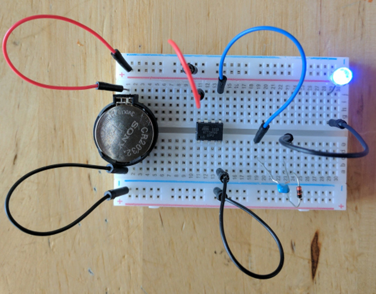
There is something deeply satisfying about making a tiny battery produce a bigger voltage. It feels a little like teaching a Chihuahua to pull a pickup truck. That is the job of a boost converter: it takes a lower DC voltage and steps it up to a higher one, allowing a modest battery, solar cell, USB rail, or supercapacitor to power electronics that would otherwise sit there looking disappointed.
The best part is that useful boost converter functionality does not have to cost a fortune. A well-chosen low-cost DC-DC boost converter can power LEDs, microcontrollers, sensors, portable gadgets, backup circuits, and small displays without requiring a gold-plated laboratory budget. The trick is knowing which corners are safe to cut and which corners are secretly holding the smoke inside the circuit.
This guide explains how budget boost converters work, how to choose inexpensive components intelligently, what design mistakes create expensive failures, and how to get reliable step-up power without turning your project into a tiny space heater. Boost converters raise voltage by storing energy in an inductor and releasing it to the output during switching cycles.
What Is a Boost Converter?
A boost converter is a type of switching regulator that produces an output voltage higher than its input voltage. For example, it can turn a 3V battery supply into a regulated 5V output, or increase a 5V rail to 12V for a small fan, LED strip, sensor module, or display.
Unlike a linear regulator, which can only reduce voltage and waste the excess as heat, a boost converter uses rapid switching, an inductor, capacitors, and a control circuit to transfer energy efficiently. The output voltage remains positive relative to ground, but it is higher than the input voltage.
The Two-Phase Magic Trick
A basic boost converter works in two repeating phases:
- Switch on: Current flows through the inductor, and the inductor stores energy in its magnetic field.
- Switch off: The magnetic field collapses, forcing current through a diode or synchronous MOSFET into the output capacitor and load.
The inductor effectively adds its stored energy to the input supply during the off phase. That is how a 3V source can help create 5V, 9V, 12V, or even a much higher voltage in specialized designs. The diode prevents the output capacitor from discharging backward into the source.
What a Boost Converter Cannot Do
A boost converter is not a free-energy vending machine. Raising voltage reduces the amount of current available at the output. If a circuit produces 5V at 500mA, that is 2.5W of output power. With an 85% efficient converter operating from 3V, the input side must supply roughly 2.94W, or nearly 1A.
That means a tiny coin cell cannot suddenly become a superhero power supply just because someone connected a cheap boost board to it. The converter can increase voltage, but it cannot create extra battery capacity, improve a weak cable, or convince a tired AA cell to bench-press a refrigerator.
Why “Rock-Bottom Prices” Can Still Deliver Good Results
Low cost does not automatically mean low quality. In many small power designs, the smartest savings come from simplifying the system rather than choosing the absolute cheapest part in every category. A compact integrated boost regulator may reduce the number of external components, shrink PCB area, simplify assembly, and prevent common control-loop mistakes.
Manufacturers offer boost-converter ICs that combine switching control, current limiting, and power switches in one package. Older low-cost controller families also remain popular because they can create DC-DC converter circuits with few external components.
The goal is not to build the cheapest converter that survives long enough for a photograph. The goal is to build the least expensive converter that works consistently under real-world conditions: low battery voltage, warm rooms, changing loads, cable resistance, startup surges, and the occasional user who plugs it in backward because life is mysterious.
Three Practical Low-Cost Paths
| Use Case | Best Budget Approach | Why It Works | Watch Out For |
|---|---|---|---|
| Quick prototype | Prebuilt adjustable boost module | Fast, cheap, easy to test | Unknown layout, ripple, current ratings, and thermal limits |
| Battery-powered gadget | Integrated boost converter IC | Small BOM, protection features, predictable performance | Follow the datasheet layout closely |
| Custom 5V, 9V, or 12V rail | Controller plus external MOSFET or diode | More flexibility for output current and efficiency | More design work and more room for mistakes |
| Mission-critical system | Qualified power design with protection | Reliability matters more than the lowest BOM cost | Do not treat this like a weekend LED project |
The Core Boost Converter Equations You Should Know
You do not need a chalkboard, a lab coat, or a dramatic soundtrack to understand the basic math. However, a few equations can prevent the classic mistake of selecting a “2A boost module” and then wondering why it becomes warm enough to toast a marshmallow.
Ideal Duty Cycle
For an ideal boost converter operating in continuous conduction mode:
Vout = Vin / (1 - D)
Where:
Voutis the desired output voltage.Vinis the input voltage.Dis the switching duty cycle.
Rearranged:
D = 1 - (Vin / Vout)
For a 3V-to-5V design, the ideal duty cycle is 40%. In the real world, losses from the switch, diode, inductor resistance, and capacitors increase the required duty cycle. Design calculations commonly include an estimated efficiency factor because the converter must supply its own losses as well as the load.
Input Current Matters More Than Most Beginners Expect
Use this quick estimate:
Input Power = Output Power / Efficiency
Input Current = Input Power / Input Voltage
Example: a 5V load drawing 500mA needs 2.5W. At 85% efficiency, the converter must pull about 2.94W from the input. From a 3V battery source, that is about 0.98A average input current.
This is why an inexpensive boost converter can work perfectly at 50mA yet stumble badly at 500mA. The output current might look small, but the input current can become large very quickly.
Inductor Ripple Current
Inductor ripple is often estimated with:
ΔIL = (Vin × D) / (Fs × L)
Where Fs is switching frequency and L is inductance. Lower inductance usually increases ripple current. Higher ripple can allow a smaller inductor, but it can also increase losses, EMI, and peak-current stress. Texas Instruments and Analog Devices both emphasize that current limit, inductance, switching frequency, duty cycle, and output demand must be evaluated together rather than as separate islands of electrical trivia.
Spend Your Component Budget Where It Actually Counts
1. Choose the Right Controller or Regulator IC
The converter IC is the traffic cop of the design. It decides when the switch turns on, when it turns off, how the output stays regulated, and how much current the circuit can safely tolerate.
For low-power products, an IC with an internal switch can be the least expensive overall choice because it reduces external parts. For higher output power, an external MOSFET controller may provide more flexibility, but it also demands better design discipline.
Some low-power regulators use pulse-frequency modulation at light loads to maintain efficiency, while others operate in continuous or discontinuous conduction modes depending on load conditions.
2. Do Not Buy an Inductor Based on Microhenries Alone
The inductor is not decorative. It is the energy-storage workhorse of the boost converter. A cheap inductor with insufficient saturation current can lose inductance as current rises, causing the switch current to spike. That can lead to poor regulation, overheating, shutdown behavior, or the electronic equivalent of a nervous breakdown.
When choosing an inductor, check:
- Inductance value
- Saturation current rating
- RMS current rating
- DC resistance
- Physical size and thermal performance
- Shielding, especially in noise-sensitive designs
Component data sheets commonly specify saturation current, RMS current, and DC resistance because all three affect real converter behavior. A standard-tolerance inductor is often sufficient, but saturation and heat margins should never be treated as optional upgrades.
3. Asynchronous vs. Synchronous Boost Converters
An asynchronous boost converter uses a diode to move energy to the output. A synchronous boost converter replaces that diode with a controlled MOSFET.
Asynchronous designs can be simpler and cheaper, especially at low output current. A Schottky diode is commonly used because of its lower forward voltage drop compared with ordinary silicon diodes. However, diode losses become more painful as current rises.
Synchronous converters can improve efficiency by replacing diode loss with a lower-resistance MOSFET path. They are especially attractive when the input voltage is low and the current is significant. The trade-off is a more complex IC and sometimes a higher component cost.
4. Capacitors Are Cheap Until They Are Not
Skipping a decent input or output capacitor is one of the fastest ways to create voltage ripple, unstable startup, random resets, or noise that makes an audio circuit sound like it is communicating with ghosts.
The input capacitor helps handle pulsed current near the converter. The output capacitor supports the load while the main switch is on and helps control output ripple. Low equivalent series resistance can be important, particularly when load current or switching frequency increases.
For budget projects, ceramic capacitors are usually useful near the IC because of their low impedance at high frequency. In higher-power or cable-fed systems, an additional bulk capacitor may help manage input transients and source resistance.
5. Select the Diode for Voltage and Peak Current, Not Hope
In an asynchronous boost converter, the diode must survive the maximum reverse voltage and peak inductor current. A diode rated only for average current may still be stressed by repetitive switching peaks. The reverse-voltage rating should account for maximum output voltage and protection thresholds, not merely the number printed on the project label.
Low-Cost Layout Rules That Prevent High-Cost Problems
Many boost converter failures are not caused by bad math. They are caused by bad layout. A physically small circuit can still create large problems when the switching loop is long, the input capacitor is far from the IC, or the high-current return path wanders around the PCB like it is sightseeing.
Keep the input capacitor close to the regulator, minimize the high-current loop between the switch, inductor, diode or MOSFET, and output capacitor, and use a solid ground path. The switching node between the controller, diode, and inductor is often called a “hot node” because it can create electromagnetic interference.
A cheap board with smart placement can outperform a more expensive board with sloppy routing. Copper is inexpensive. Debugging at 1:30 a.m. is not.
Protect Your Boost Converter From the Problems It Cannot Magically Solve
Input Sag
If the battery, USB cable, solar cell, or bench supply cannot provide enough current, the input voltage will sag. The boost converter responds by drawing even more current to maintain output power. That can cause brownouts, oscillation, thermal shutdown, or a loop of sadness where nothing powers correctly.
Output Short Circuits
A basic boost topology can be vulnerable during output short-circuit conditions because the input-to-output path is not as naturally isolated as some other converter topologies. Use a regulator with current limiting and protection features when possible, and consider a fuse, load switch, or alternative topology for designs exposed to harsh faults.
Thermal Overload
Heat is rarely a surprise. It is usually a math problem that was ignored until it became a smell problem. Check the IC package thermal limits, diode or MOSFET losses, inductor DC resistance, and PCB copper area. A component that survives on the bench for five minutes may still fail after an hour inside a sealed plastic enclosure.
Example: A Budget 3V-to-5V Boost Converter
Imagine a small battery-powered sensor project that needs a stable 5V rail for a microcontroller module and a low-power display. The expected load is 300mA, with brief peaks near 500mA.
A practical design process would look like this:
- Define the true input range, such as 2.7V to 3.3V rather than simply “3V.”
- Design around the worst case: 2.7V input and 500mA output peak.
- Estimate output power at 2.5W and input current above 1A at lower battery voltage.
- Select an IC with sufficient switch-current margin, not merely a 500mA label.
- Choose an inductor whose saturation-current rating exceeds the expected peak current.
- Use input and output capacitors recommended by the regulator data sheet.
- Check temperature after sustained operation, not just startup.
The final circuit may only use a regulator IC, inductor, capacitors, feedback resistors, and perhaps a diode. That is the beauty of boost converter functionality: the component count can be small, but each component must do its job properly.
When a Boost Converter Is the Wrong Tool
A boost converter is excellent when the input voltage is always below the required output voltage. But if the input can be above or below the target rail, a buck-boost converter may be more appropriate. For example, a battery pack that ranges from 3V to 4.2V cannot reliably produce a tightly regulated 3.3V rail with a boost-only topology.
Likewise, if you need isolation, protection from difficult short-circuit conditions, or multiple output rails, a flyback, SEPIC, or other power topology may be worth the additional cost. The cheapest boost converter is not a bargain if it is solving the wrong problem.
Conclusion: Cheap Boost Converter Functionality Is About Smart Trade-Offs
Boost converter functionality at rock-bottom prices is absolutely possible when cost savings come from smart architecture, integrated components, efficient layout, and realistic power expectations. The best low-cost design is not necessarily the one with the smallest bill of materials. It is the one that delivers stable voltage, stays cool enough, survives normal faults, and does not require a support group after testing.
Start with the real input-voltage range, design around the maximum output load, choose an inductor with proper current margin, use capacitors that can handle ripple, and treat layout as part of the circuit rather than an afterthought. Follow those rules, and even a modest boost converter can deliver surprisingly capable, reliable power.
Practical Experiences With Low-Cost Boost Converter Designs
The following field-style experiences reflect common lessons engineers, makers, repair technicians, and hobbyists encounter when working with low-cost boost converter boards and simple custom designs.
Experience 1: The Module That Worked Until the Load Arrived
A low-cost boost module often looks impressive during the first test. Set the output to 5V, connect a multimeter, and everything appears perfect. The voltage is clean enough, the adjustment screw feels satisfyingly professional, and for about thirty seconds you believe you have defeated physics.
Then the real load arrives. A Wi-Fi board starts transmitting, a motor kicks on, or a display backlight wakes up. Suddenly the output falls to 4.2V, the module becomes warm, and the microcontroller resets every few seconds.
The usual problem is not that the module is “bad.” It is that the current rating was interpreted as output current without considering input current, efficiency, heat, and transient load demand. A boost converter supplying 5V at 1A may need far more than 1A from a low-voltage battery source. The cure is simple but unglamorous: calculate the input current, test under the real load, and leave current margin.
Experience 2: The Inductor That Looked Fine but Was Not Fine
Inductors are sneaky. Two parts may both say “10 µH,” yet one can handle a healthy boost converter current while the other saturates early and turns the circuit into a tiny electrical drama production.
In one common scenario, a project uses a bargain inductor selected only by inductance value. At light load, it works. At higher load, the regulator starts clicking, the output ripples, and the switch-current limit activates repeatedly. Replacing the inductor with one that has a higher saturation-current rating often fixes the problem without changing the IC or output capacitors.
The lesson is brutally simple: inductance value is only one chapter of the story. Saturation current, DC resistance, RMS current, and temperature rise are the rest of the book.
Experience 3: The “Bad Battery” That Was Actually a Bad Cable
A boost converter can expose weak wiring faster than almost any other small circuit. A USB cable with thin conductors or a battery holder with weak spring contacts may drop enough voltage under load to make the converter unstable.
The suspicious symptom is usually this: the converter performs well from a bench supply but fails from the intended battery pack. The first instinct is to blame the battery. Sometimes the battery deserves it. Other times, the wire resistance is stealing voltage before the converter even gets a chance to work.
Measuring voltage directly at the converter input under load is the fastest reality check. If the input supply collapses from 3.3V to 2.5V during a current spike, the boost converter must pull even more current to maintain output power. That can create a feedback loop of worsening performance.
Experience 4: The Noise Problem That Was Really a Layout Problem
A prototype on jumper wires may function electrically while behaving like a tiny radio transmitter. The output is correct, but an audio amplifier hums, a sensor reads strange values, or a nearby radio module loses range.
Moving the input capacitor closer to the regulator, shortening the high-current loop, adding proper grounding, and reducing the exposed switching-node area can make a dramatic difference. The amusing part is that the schematic does not change at all. The circuit becomes better simply because the copper starts behaving itself.
Experience 5: The Cheapest Reliable Upgrade Was Protection
Inexpensive boost converter projects often skip protection because “it is only a small board.” Then someone accidentally shorts the output with a test lead, reverses a battery, or connects an unknown load with a giant startup surge.
A current-limited IC, input fuse, reverse-polarity protection device, or output load switch may add a few components, but it can save the entire board. In many practical designs, the cheapest reliable improvement is not a fancier regulator. It is one modest protection feature placed in the right location.